Last time we looked at configuring an op-amp with negative feedback, but with enough reactive (phase shifting) components to make it unstable. The trouble with the amplifier of choice is that it’s a very low-bandwidth part, intended for use amplifying slow or nearly DC signals. The size of components required to cause instability in this case is impractically large, so we must switch to an amplifier with a much higher bandwidth.
Try it
The previous example is a good theoretical illustration of intentionally causing oscillations, but it’s a little impractical to build. Repeating the inductance equation here:
![]()
If the feedback resistors are 10KΩ, L turns out to be nearly 16H! A Henry (unit of measure for inductance) is really big; most PCB-mountable inductors are in the micro- or nano-Henries. Even an inductor in the milli-Henries is physically unwieldy.
Reducing the resistors to 1KΩ will bring inductance down to ~1.6H, but that’s still quite large. Increasing the frequency to 10KHz would help a lot, but we’re still looking at ~1.6mH, and the MCP6441 is not made for this; the frequency is already greater than the gain-bandwidth product (9KHz), so it won’t work.
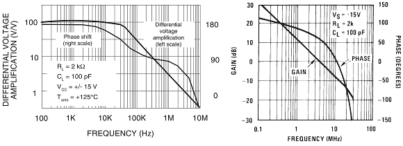
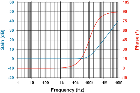
With a higher-bandwidth amplifier, these values become a little more obtainable and can be dropped onto a breadboard for testing. For example, if we move to an LF353, with a GBP of 4MHz, we find first of all that the three manufacturers who make this product either do not include plots, or their plots have peculiar labelling, and in short, look wrong. Here’s how it breaks down: TI has two products, and LF353 and an LF353MX. The data sheet for the vanilla LF353 does not include any plots. The datasheet for the LF353MX on the other hand, does. Here’s ST’s (left) and TI’s (right) view of the gain & phase vs. frequency:
The following is more editorial than should be allowed; sort of a stream-of-consciousness of datasheet interpretation…
Notes (Beware! Datasheets are never free of errata; but then, neither are blogs):
- These diagrams have never been updated, and look to be copied from their decades-old datasheets; not that this makes them wrong, but a more accurate representation of behaviour is easily produced at this time. They are wrong for other reasons.
- Both show open-loop performance with a 2KΩ, 100pF load, though ST for some reason feels an ambient temperature of 125°C is the most likely one for which operating parameters are required.
- ST indicates the Y axis of their plot is Differential Voltage Amplification (V/V) which we must assume is Vo/ΔV and is really a ratio of V:mV as the typical large-signal gain is -from their parameter table- 200,000:1, not 100:1. This is further confused by their large signal gain curve showing it’s 200:1 at around 25°C, and 60:1 at 125°C…but the above curve shows it’s around 100:1 at 125°C…huh? This is obviously wrong. If that weren’t confusing enough, a gain of 100 should really be 100,000:1, which when converted, turns out to be 100dB! This implies the curve really already has a log scale, but then 0dB is not on the plot, which is an absolute requirement, so that can’t be right. Looking at the fragment provided in TI’s datasheet, their 0dB line corresponds -approximately- to the line on the ST datasheet marked with a 1, but we don’t know the temperature to which TI’s datasheet corresponds. If 1 really is 0dB, then 10 must be 20dB, and 100 must be 40dB…huh? That can’t be right either. If 100 corresponds to 100dB, and 10 corresponds to 10dB…no that doesn’t work either. This plot is terrible! What should it look like? If the figure showing the gain is 60:1 at 125°C, which we must interpret as 60,000:1 because it’s mislabelled too, the gain comes out at ~96dB. You just have to try it on a breadboard.
- Whereas TI’s diagram includes only a small portion of ST’s, showing only the gain rolling off between 100KHz and 30MHz, ST’s covers 100Hz to 10MHz. In fairness, TI provides a separate chart of open-loop frequency response, but does not include phase, and the curve shows 110dB up to 10Hz, whereas ST’s above shows ~100dB up to 30KHz. One must ask, are these the same part?
- ST’s diagram indicates that frequencies below 10KHz, phase shift is 180°, so this amplifier will oscillate no matter what; but, it does not. TI’s fragment shows phase heading north to 180°, but since the destination isn’t shown, we can’t say.
- ST indicates 90° phase shift at about 300KHz; TI indicates 90° phase shift at about 600KHz.
- ST indicates 0° at ~6MHz; TI indicates 0° at ~10MHz.
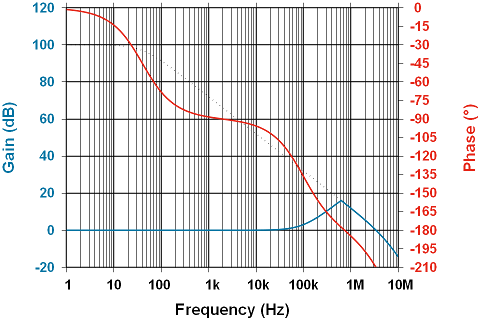
After a little testing, the amplifier’s large signal behaviour looks much more like this:
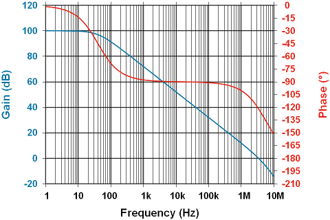
Note the phase bears only a passing resemblance to the data-sheet. Don’t believe it? Try it with a real device:
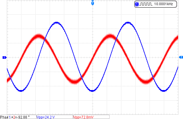
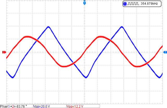
- The red curve is ΔV; the blue curve Vo.
- The supply voltage to the amplifier is ±15V.
- The amplifier is in an open-loop configuration; no feedback.
The phase shown on the ST data sheet should be close to 160°, but Vo is clearly lagging by 90°, so the angle would be -90°. Note also the input and output peak-peak voltages. Working this through shows only 50dB of open-loop gain at 10KHz; not quite what the manufacturer says, but interestingly spot-on in TI’s datasheet (Open Loop Frequency Response figure).
Closing the feedback loop with unity gain, we should be able to see the phase error increase as we approach the unity gain bandwidth frequency:
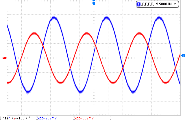
Note the amplitude here is much much lower. Since its configured for unity gain, the input amplitude is actually 7Vpp. More importantly, the phase lag from ΔV to Vo is sitting pretty close to 135° at 5.5MHz input.
That aside, the amplifier was configured as in the last post, but included the test load specified in the manufacturer’s datasheet (2KΩ in parallel with 100pF):
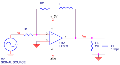
With 10KΩ resistors in positions R1 and R2; the inductor chosen was 1000μH. This did not produce the oscillations expected. It turns out the amplifier is quite able to deal with the inductance in its feedback path. After some careful checking, it turns out a much lower feedback resistance, R2, is needed: 620Ω does nicely. Below is the impedance over frequency, including phase:
As previously discussed, the positive phase actually pushes the amplifier towards 180°. Here is what the final gain/phase curve looked like:
Note the gain is increasing with frequency as we approach the unity gain curve, resulting in a rate of closure of 40dB/decade, which just happens to coincide with the phase reaching -180° where the curves meet. Applying power to this results in some very strange looking waveforms:
There is no input connected to this, so the amplifier is doing its own thing here. Note that the red trace is what’s on the inverting input; so much for ΔV = 0 at all times! Oscillating at ~355KHz, it’s probably affected by a bit of stray capacitance in the breadboard and the components around it, but those are a little tough to measure accurately. So why does it look like an ugly triangle-wave, and why is the phase angle not 180°?
Previously, in the discussion of decompensated amplifiers, slew rate was touched on: the maximum rate at which the output can change. The LF353’s is between 12 and 16V/µS, meaning that’s how much its output can swing per microsecond. This can be roughly measured from the above scope capture by inverting the oscillation frequency, halving it, and dividing that into the peak-to-peak swing voltage:
![]()
It’s nearly exactly where it’s expected to be.
As to phase, the capture shows -83.76°, but this is actually bouncing around quite a bit; it’s unstable! The amplifier is unable to cope with the signal it’s feeding back on itself. Slew rate limiting is actually masking the phase error inside the amplifier, which is very clearly sitting somewhere near 180°. It wouldn’t oscillate otherwise.
Introducing extra phase delay to the feedback path is really the hard way of doing it; it would be much easier to use positive feedback -connecting the output to the non-inverting input- as the 180° phase shift is accomplished without reactive components, though it won’t oscillate without some additional coaxing.
Next time, we get to the basics of filtering.
References
- STMicroelectronics – LF253, LF353 – Doc ID 2153 Rev 3 – March 2010 – Figure 10
- Texas Instruments Inc. – LF353 Wide Bandwidth Dual JFET Input Operational Amplifier – SNOSBH3D – May 2004 – Figure 13
- Microchip Technology Inc. – MCP6441/2/4, 450nA 9KHz Op Amp – DS22257C – 2012 – ISBN 978-1-62076-244-8