Moving from concept to reality
After completing the schematic and bill of materials, preferably the enclosure design too, a project reaches the stage of PCB layout. The bill of materials and a list of wire connections – aka netlist – are used to physically place the components on a surface; or, on two surfaces if using both sides of the PCB.
At this stage compromise enters the design. A schematic is an ideal representation of the circuit, but does not touch on physical reality.
What could go wrong?
- Components may be too big to fit the available PCB area;
- A completed enclosure design will include a space-envelope into which all components must fit, but they may not;
- Connector locations specified in the enclosure design may look great in that 3D CAD model, but the connector bodies inside the enclosure may not fit close enough together to protrude in the right places;
- Connectors on a PCB will all rest against the PCB, meaning they may not sit in the most desirable place, possibly leading to a requirement of internal cabling and further restrictions to the available space-envelope;
- If the components inside the case consume substantial power, they will get hot; that heat needs an escape route;
- Consuming or delivering substantial power may force a requirement of wider traces on the board, restricting the available area for components;
- High-voltages may raise safety concerns and require larger clearances than originally anticipated;
- In order to achieve desired performance, analogue sections should ideally be placed as far away from noisy digital circuitry, clock oscillators, and switching regulators as possible;
- If there are clock oscillators on the design (always!) testing may be required to verify the product does not transmit radio interference unintentionally; surpises here lead to adding filter components to dissipate rather than radiate that energy, leaving the design with less available physical space for routing.
The above list is not exhaustive; this is a complicated area requiring much attention to detail.
Density
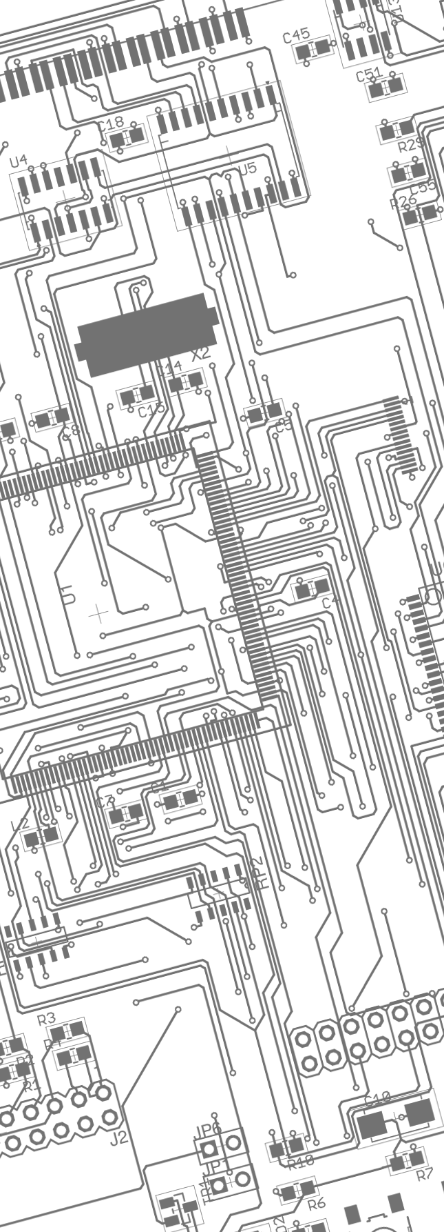
One way of increasing component density on a board without increasing physical size is to use both sides, an effective strategy if not pushed too far. Double-sided boards are harder to route; there is much less available area for traces and vias, not to mention reference designators showing which site is for which component. Designators can be forgone in production, saving a few pennies in board cost, however it does make for a more difficult product to debug should problems arise.
If using both sides is not enough, the next step is to increase layer count. Jumping from two layers to four is a very big expense, as the PCB fabrication technique is quite different from a vanilla two-layer board. Jumping from four to six or more may not be as big of a cost hit as that first leap, as the construction techniques for higher layer count boards are similar regardless of how many layers are used.
Vias can become a source of greater complication in multilayer boards too. In a two layer board, a via passes a signal from one side of a board to the other, but in a four-layer board, vias may be blind. That is, they could go from an internal plane to only one side of the board. If more than four layers are employed, yet another layer of complexity arises: buried vias. These may traverse one internal board layer to another without ever reaching an outer one. This can allow for considerably greater density of routing, but nothing is free. Aside from the literal meaning – more dollars will be spent – vias still block possible passage ways for traces on a board, and will make routing more difficult, even if blind and/or buried.
Unintentional Radiator
All of that speaks to the mechanics of increasing density, but there are other concerns for the layout designer. Signal paths that enclose a significant cross-sectional area will radiate energy if any measurable current flows around the loop. For this reason, the choice of routing a long distance around an obstacle without passing a signal from one layer to another may cause more trouble than expected, as more area will be enclosed by the signal path. Dropping a via to jump over or under an obstacle will usually be the lesser of two evils.
If that weren’t enough, a basic principle where current is flowing is that it will return on a path enclosing the smallest possible area. This means, for instance in the case of a board with a ground plane, current that flowed through a trace will return through the ground plane exactly underneath the trace it flowed in. If this is not possible due to vias and other obstacles, a larger area will be enclosed leading to more unintentional radiation of energy. A good designer will spend the time making sure that current return paths are as close as possible to the originating paths.
Exotic Traces
Where high-frequency transmission of signals is concerned, impedance matching may be required to the point of controlling impedance between both traces and ground, and traces and each other. A board fabrication shop will usually be able to help with this, as it’s a capability found only in premium layout tools. As the requirement to communicate at the limits of copper traces becomes commonplace, impedance management capability will undoubtedly become available in more budget conscious layout tools.
Materials
Most fibreglass PCB material today is 94V0 rated. This mysterious term just means the board won’t burn if something goes wrong; the more commonly used term is self-extinguishing. If a component failure producing extreme heat occurs, the board may get hot enough to ignite the resin used to bind the fibreglass together. A 94V0 rated PCB will char, smoke, and smell delicious when this happens, but it will not burn. This rating is mandatory for anything connected to the telephone network, and in many other areas where human safety is concerned.
With the growth of high-lumen LEDs, Aluminium PCBs have become much more common. Aluminium PCBs become part of the heat dissipation mechanism for these designs, however they’re limited to single sided with no vias. This means usually that the control circuitry resides on a conventional PCB, and only the LED itself is mounted to the Aluminium substrate PCB.
Phenolic resin PCB is still commonplace in consumer electronics because it’s cheap cheap cheap…did I mention cheap? It’s use is limited because it does not support plated through-hole, so no vias, and is virtually always signle-sided. More subtly, it has a much greater coefficient of thermal expansion as compared to fibreglass, and for this reason can’t work with high-density components.
Flexible (mylar) PCB is found on devices such as LCDs where is a small amount of circuitry is on the connector cable. This is handy for space restrictions, but usually only used in high-volume manufacture.
Current Capacity
When a PCB is tasked with conducting high-current, such as in the operation of high-brightness LEDs or motor drives, current may creep up into the amps. In this case, concerns about the traces themselves burning up arise. The easy fix is to widen the trace. There are charts available, applications for download, and even on-line temperature calculators for figuring out how much the trace temperature will rise above ambient.
Most calculators provide repeatable results, however this only works if the trace hasn’t lifted off the board. When copper is flowing high current, some of the heat produced does dissipate into the fibreglass PCB. If the trace has lifted off the board due to repeated heating/cooling cycles, it will not be able to dissipate heat, and will burn. The simple rule is, don’t push your luck; be generous where high current is flowing.
If the extra width doesn’t meet the design goals, the next move is to increase the copper weight. A slightly mysterious term is used to describe copper thickness on a PCB. The most common weight is 1oz. What this means is, if the PCB was plated completely on one side over a 1 square foot surface, the amount of copper used would weigh 1oz. If the weight is doubled to 2oz, the traces are much thicker, can handle considerably more current, and don’t need to be nearly as wide. Heavier weights are available too. As with all things exotic, ya wanna play, ya gotta pay. If board size can be increased to accommodate the wider traces at 1oz, this is often the less expensive solution.
An example of high-current design without opting for higher-weight copper can be seen in the DC UPS design featured under consulting examples, the circuit board can have in excess of 50 Amperes flowing through it during the initial stages of a power failure. A close look at the PCB mounted to the enclosure door should show traces over 50mm in width.
Design Rules
“Design rules” is a generic term that usually encompasses three things:
- Minimum trace width
- Minimum space between traces
- Minimum via diameter
There are several other parameters that come up, such as permissible proximity to PCB edges, but the above three parameters are usually the first thing a fabricator will seek. As equipment improves, the minimums defining these rules become smaller. Fifteen years ago 8/8/20 (0.008″ trace, 0.008″ space, 0.020″ diameter via hole size) was the norm, but as of this writing it’s 7/7/16 locally, and even tighter elsewhere. Tighter rules are easily specified, but the above represents the point on the price curve where the design moves from standard to exotic; the mapping of price to those two terms should be self-explanatory.
Design for Manufacture
High-speed placement machines usually need a way of registering where the board is in relation to turret doing the placing. Otherwise, how can that uber-high density BGA package you just design in be guaranteed to land in the right spot on the board? A fiducial is a small marker with a known relationship to the high-density component site. Once the placement machine has found the fiducial(s) it can reliably drop the part onto the board. For smaller boards, two fiducials on each side can easily provide enough resolution to guarantee reliable assembly; larger boards with many high-density components usually go through assembly with less hassle if they have a set of fiducials per component. This applies to large QFN, and BGA packages in particular.
If volume production is the final destination of a design, it may be worth while to think about how the product will be tested as it rolls of the assembly line. Quality Assurance is a market differentiator, and if a product can be fully tested prior to shipping, less returns means much less expense for the producer.
Bed-of-nails testing is a common way of testing boards rapidly. This system works by placing the board into an assembly where probes are pressed against it so signals can be driven through it to verify functionality. The ability to work with a bed-of-nails system must have been considered early on in the design cycle, preferably at the schematic stage. Less obvious details, like adding resistors in series with enable/disable pins is also a good idea. This allows the test equipment to overrule any processor on the board. For example, if an oscillator has an enable/disable pin, the space-conscious designer would just hook it up to the supply rail, but then the test equipment can’t control the oscillator. Adding a series resistor to that connection fixes the problem.
Regulatory Compliance
This comes up with greater force depending on how directly a product will reach a consumer. Industrial electronics do not escape approval requirements; however, the rules are generally a little more lax because products are being used by experts rather than consumers who may not wish to concern themselves with details.
- Is regulatory approval for unintentional radiators (FCC part 15A or 15B) required by this design? If so, many precautions must be taken to ensure that the design will not radiate noise at a level exceeding guidelines set by governing bodies.
- Is there a danger of fire? The PCB material employed may need to be of a self extinguishing nature.
- Will the board be subject to static discharge? If so, precautions must be taken to protect the input stages from being destroyed in the course of normal operation.
- Is there a telephony interface on the design? If the board must ultimately connect to the telephone network, the design must ‘fail’ safely in the presence of a line surge or lightning strike. The translation is that the board may not catch fire or leave the connection to the Central Office (CO) in an off-hook state.
Examples
Some illustrations of printed circuit board layouts are shown below. Each example depicts a different type of design expertise typically employed in our design process.
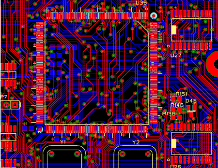
A CPU layout from the core of an embedded monitoring system.
Above is shown a section of a CPU and surrounding connections. Most designs with pitch this fine will require at least four layers to route properly. Four layers is preferred in these cases as there are less problems with unintentional radiation of RF energy, or EMI. EMI is generally a problem where severe impedance mismatches occur, and extremely fast rise and fall times of digital signal lines are encountered. A specific example of a consistent problem in high-speed designs like the one shown above is that of clock oscillators used to drive the chip itself. Traces coming from oscillator drive pins should be kept as short as possible, filtered (again, if possible), and kept as far from other traces as is reasonable.
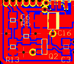
RF Input Stage
At left is shown a portion of an RF input stage for an embedded servo controller. In the case of RF input and drive stages, a well drawn schematic can be invaluable in determining what is important in the layout. Generally, these types of stages are linear in nature, meaning not that there are second or higher order effects taking place on transmission lines, but that the components are laid out in stages, each one feeding into the next. This means components can be oriented such that traces are as physically short as possible and use few, if any, vias. This can give some designs the appearance of being all components and copper planes, with very little in the way of visible traces. In the RF stage shown at left, the antenna connection to the design (the outermost pin in the upper left corner) passes through a filter stage and into a discrete amplifier. Most traces are shorter than the components themselves.
J-Tech Engineering is always pleased to discuss layout requirements for your designs. We enjoy partnering closely with our customers to produce the most effective designs possible; your successes are viewed as our successes. Please see the company information page for contact information.