Last post we examined the Sallen-Key topology, now we get into a specialty device, namely the instrumentation amplifier. Typically constructed from several amplifiers, it has proven so effective in amplifying low-frequency differential voltages, it’s now widely available in pre-packaged form. In this case the signal being amplified is of very low frequency:
fsensor < 100Hz
Owing to this, gain can be set quite high, in some cases approaching open-loop.
Instrumentation Amplifier
In the discrete implementation version, this circuit takes the generalized form:
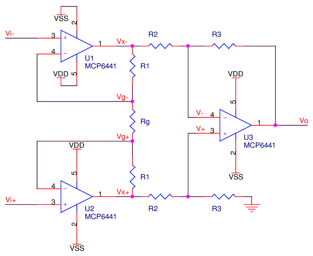
The choice of MCP6441 is appropriate, as it’s a very low-bandwidth amplifier, perfect for the job. Note however that its open-loop gain begins to drop off at well below 1Hz, so for rapidly varying signals it’s a poor choice.
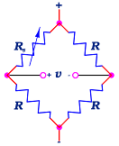 Where does this get used? The Wheatstone bridge (shown at left) is a standard means of converting a resistive sensor under measurement into a voltage. Many sensors are devices that, by design, change their resistance in relation to the property being measured. Pressure sensors, load cells (also a pressure sensor), resistance temperature devices (RTDs), light sensors (aka photocells), are all examples. One or more of the bridge resistors are replaced with the sensor. Pressure sensors often replace all four resistors with sensing elements to boost sensitivity and repeatability. Usually these devices only change their resistance by tiny amounts, so a great deal of gain is required to make the sensor’s behaviour observable.
How does it work? The amplifier’s performance can be explained without frequency domain analysis, Bode plots, or scope captures. The signals at Vi+ and Vi- are connected to the inputs of op-amps U1 and U2; the only current in is what goes into the non-inverting terminals: effectively none. The inputs have very little effect on the measurement sensor, and the very high input impedance terminals can be treated as ideal. The inverting terminals of the two amplifiers can be assumed to match the non-inverting inputs, so Vi- and Vi+ appear on the top and bottom of the gain resistor, Rg. The two amplifiers’ outputs (Vx+ and Vx-) feed back through their respective R1 resistors, and since there’s no place else to go -the inverting inputs take approximately no current- all current (Ig) must flow through Rg and both R1 resistors. The voltage across Rg will therefore always be equal to Vi.
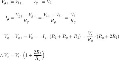
The value of Rg will in turn dictate how much current flows between the op-amp outputs, which sets the amplitude of two amplifier output pins, and thus the gain! The relationship is upside-down, so a higher Rg will result in a lower gain, and vice-versa. Because the two instances of R1 are conducting the same current, each will develop an identical voltage, which will appear at the outputs of the two amplifiers on the left. The gain relationship works as follows:

It is fairly standard to set the final amplifier’s (U3) gain to unity, so:
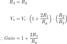
…which is the simplest way of expressing the circuit’s behaviour.
Since the input terminals of U3 each have identical resistances (R2 in parallel with R3; so says Thevenin), the inputs are perfectly matched (see the input stage posting for an explanation of why this is important). This means the third op-amp will experience no offset. The top instance of R3 connects to the output, a virtual ground, the bottom one to physical ground.
In its purest form, the value of Rg sets over-all gain, but more can be had by making R3 > R2. If the property being measured has a frequency component, there is an advantage to using Rg for only some of the gain, and the ratio of R3/R2 for the rest. Spreading around the gain reduces the risk of amplifiers hitting their gain bandwidth product limit, allowing the circuit to handle a little higher frequency.
Source of Error
The phrase “perfectly matched” should send prickling sensations up and down the weary designer’s spine; nothing is ever perfectly matched. If the resistors used for R1 do not match precisely, the voltage developed at the two output terminals will have a gain mismatch error, causing the common mode voltage to be affected by the input amplitude. Resistors used for both R2 and R3 must also be precisely matched, but since there’s no gain in this stage, the bigger danger is an offset voltage creeping into the output.
So how does one mitigate these risks? The obvious choice is to pick resistors with sub-1% precision and very low temperature coefficients. This is a good start, but a little pricey. An oft’ overlooked possibility is to design with multi-resistor surface mount components. Multi-resistor packages may have a tolerance of 1% or even 5%, but the difference between one resistor and the next within the package itself will be exceptionally small. The variation of all resistors in the package is less critical than the variation of resistors relative to each other, and their respective temperature drift can be tolerated so long as they drift together, also very likely. Conveniently these packages are also physically quite small.
If building with discrete amplifiers, the above considerations should make for a robust design, but there’s an easier way. Since the circuit is so common and popular, it’s available in a variety of integrated packages, such as TI’s INA118:
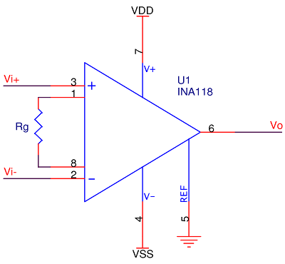
It looks like a single instrumentation amplifier, but it really is three op-amps in one package with internal precisely matched laser-trimmed resistors; gain is set only by Rg.
REF Pin
The reference pin should be, in a dual-supply configuration, connected to ground. Its impedance should roughly match the virtual impedance of the unity-gain amplifier, so if there’s a 50Ω source impedance, connect a 50Ω resistor to ground, unless the datasheet says otherwise. This may not yield a measurable improvement in performance. So why not just call it ground if that’s its purpose?
In a single-supply circuit, such that VDD is say +5V and VSS is ground; hooking the REF pin to ground is like hooking the non-inverting impedance path to the negative supply rail rather than what the op-amp treats as ground. Ideally something that looks like VDD/2 is what is required.
Do not just use a voltage divider from VDD to ground. Although the VDD/2 voltage is a close match to virtual ground, its impedance is ½ that of the two resistors used to split the voltage; it needs to be a low-impedance path to work properly, otherwise the amplifier can pick up noise, and there’s that offset problem. One approach is to use an amplifier configured for unity gain with a voltage divider on its non-inverting input. The output will match VDD/2 but will have the same impedance to ground; this makes using a quad-amplifier IC for a discrete implementation a great solution.
Note that in the case of the INA118, the manufacturer recommends grounding the pin even in single-supply systems, and further recommends that no source impedance, like the 50Ω mentioned above, be used.
Common Mode Caveat
There is yet another danger with instrumentation amplifiers. The common-mode voltage (or average) on the inputs, (Vi+ + Vi-)/2 is an important number. If running with dual supplies, inputs should be centred about 0; if single supply, they should be centred at roughly mid span, however some experimenting should be done to guarantee performance. Why does this matter? Gain is extremely high on the input stages, and Vx+ and Vx- will be centred about the common mode input voltage. Suppose, in a single-supply system with VDD=5V, the inputs have a common mode voltage of 1.0V; the amplifier will attempt to drive Vx+ or Vx- below the negative supply rail, but it cannot and will instead merely approach 0V. The output voltage will not accurately represent the input.
The above discussion pertains to the discrete implementation. If working with an integrated instrumentation amplifier, check the common mode range! Below is a graph appropriated from TI’s INA118 datasheet illustrating the problem:
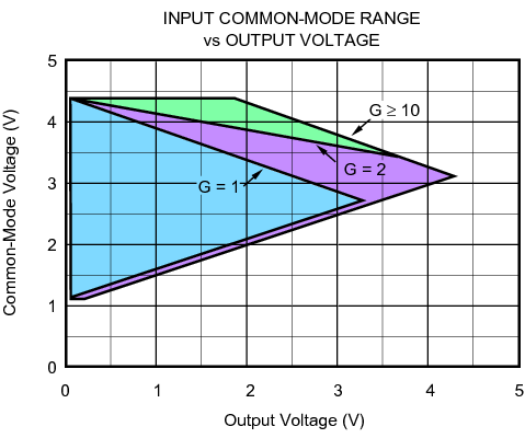 The above plot applies to a single supply configuration with VDD=5V and various possible gain settings. If the common mode voltage at the inputs is 1V, the amplifier will not produce ANY output. The best case scenario is to have the common mode voltage somewhere above mid-span, the idea being to allow the output voltage to climb as high as possible, and hence maximize useable range. If gain is set to two or more, it is best if:
3.0V < VCommonMode < 3.5V
This is not obvious without looking at the graph, and in fairness the part is much more tolerant of common mode variations in dual-supply mode.
Wrapping up, a designer should be able to put together a sensor amplifier with ease based on the above discussion. One is easily built from scratch, or can be had completely integrated. The issue with common mode voltages is worth noting too.
References
- INA118 Precision, Low Power INSTRUMENTATION AMPLIFIER, SBOS027, Texas Instruments.