 This series of posts explores fundamental op-amp design issues; why in some projects tough problems never turn up, yet in others they create insurmountable obstacles. The simplest op-amp circuits or design requirements can keep a designer away from the non-ideal features of op-amps, but sooner or later, all those tables of obscure numbers in the op-amp’s data sheet must be understood in order to make it work.
Operational Amplifiers are one of the coolest inventions in electronics. Processor and FPGA fans can disagree, but there’s room for more than one cool thing out there. Processors make it possible to skip over a lot of tricky, arguably elegant work in hardware design, but at a price: many hardware engineers struggle with analogue design, not out of inability, but from a dearth of opportunities. As the saying goes, “good judgement comes from experience, and a lot of that comes from bad judgement.” (wish I could take credit for that fine aphorism, but credit to Will Rogers)
This is the world of gains, offsets, filters, Bode plots, poles & zeros, gain bandwidth products, and impedance matching. Turning to a circuit simulator like SPICE can lead a designer in the right direction, but simulators work in a rarefied world; simulations do not always align with reality.
Hardware is messy. Stray noise, stray capacitance, stray inductance, trace-to-trace coupling, bizarre field interactions, among many others are, well, pick a metaphor: flies in the ointment; ghosts in the machine; Murphy’s Law; monkeywrenches; gremlins. All of these things and more can make working with a simple op-amp a very frustrating experience.
Complex amplifier circuits don’t come up often, but simpler ones are more common than one might expect. In our embedded design business, it’s rare to not have at least one in a design. They’re essential for transforming obscure signals into robust ones easily read by a processor.
A Real-World Example
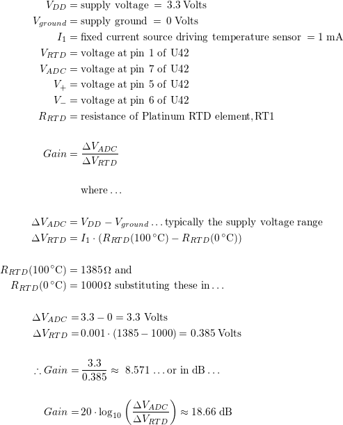
Take interfacing a temperature sensor, essentially a resistor with a value dependent on temperature, to a processor. For simplicity, we’ll assume the whole system runs at 3.3V. A typical Platinum RTD sensor has a resistance of 1000Ω at 0°C, and a temperature dependence of 3.85Ω/°C. If a fixed 1mA of current is driven through it, 1V at 0°C will be seen across it, but over a typical temperature range, say 0-100°C, the resistance will change by 385Ω, with the voltage sitting at 1.385V. If a processor’s internal ADC has 10-bits of resolution, thus dividing 3.3V into 1,024 quantization levels, each step is ~3.22mV, so the values read by the ADC will vary from 310 to 430. Using this range for any sort of calculation would mean that the measurable resolution is 0.837°C/quantization step, or ~1.5°F/step; pretty coarse. It would be far more useful if the voltage presented into the ADC’s input varied from 0V to 3.3V across the temperature ange of 0°C to 100°C, given it’s the temperature range of interest. This is where an operational amplifier comes in.
An amplifier can be used to offset the 1.0V at 0°C, placing at at 0V. The very same op-amp can employ a little gain to take that 1.385V, which would now be 0.385V, and multiply it by a factor of ~8.6, thus putting the voltage at 100°C at ~3.3V. Now the 1,024 steps of the 10-bit ADC are spread over 100°C, meaning the resolution has now gone from 0.837°/step to 0.0977°/step! Not bad for a single component with a few passive devices wrapped around it.
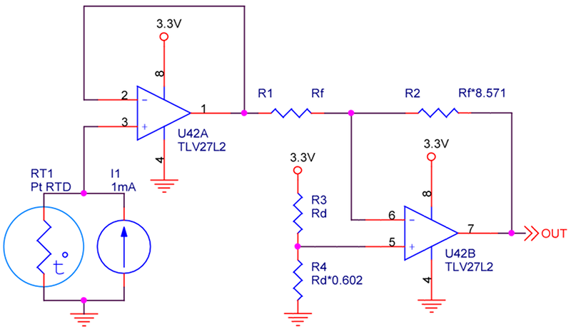 The above figure is oversimplified, but illustrates the concept. The op-amp on the left is configured as a unity gain buffer, and is present for two reasons: 1. provide a copy of the voltage across the RTD element, but with a low source impedance; and 2. isolate the RTD element from the op-amp on the right. If the unity gain buffer were not present, current from the amplifier on the right would pass through the RTD, introducing an error in the temperature measurement.
The circuit output is inverted, so 0V corresponds to 100°C, and 3.3V corresponds to 0°C. This is could be inverted in hardware, but it’s a simple matter to invert the conversion results in a processor, not to mention cheaper than more hardware. The upshot of all this is we can focus on the amplifier on the right, the one transforming the sensor’s resistance into the full voltage range of the fictitious processor’s ADC input. First, work out how much gain is required:
The two feedback resistors, R1 and R2, realise the gain required to amplify the voltage coming from the sensor:
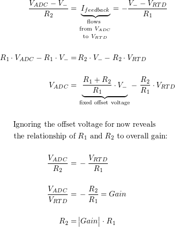
Note the resistor relationship involves an absolute value, as resistors with negative resistance are just slightly unusual.
From here we move on to setting the offset value. Ideally, the temperature range would be centred at 1/2 the supply voltage, or 1.65V. This would make all of the arithmetic easy, because the voltage would be centred at mid-span of the supply, and there is very little to calculate. Instead, it is centred at 1.1925V, somewhat below a point at which the full temperature range can be seen. In order to shift the output so that it covers 0-3.3V as desired, the non-inverting terminal (pin 5) of U42 must be set to a voltage that, when combined with the gain, positions the extremes of temperature being measured at the extremes of supply voltage. A little arithmetic shows that this is possible, and fairly straight-forward:
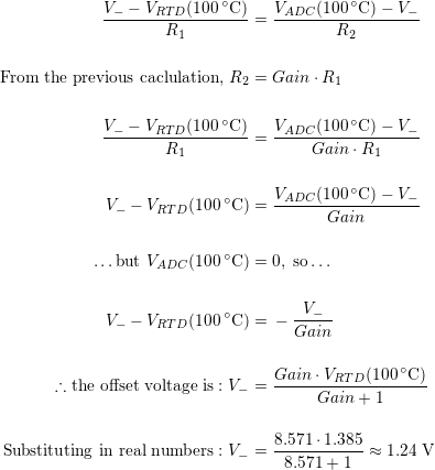
Now all that’s left is to work out the relationship between R3 and R4. The voltage at the inverting input to the op-amp will (ideally) be the same at the non-inverting terminal:
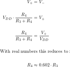
If you simply must see this in action, here are some commercially available resistor values:
- R1 = 4.7KΩ
- R2 = 40.2KΩ
- R3 = 11.3KΩ
- R4 = 6.81KΩ
It would be instructive to build this on a breadboard; but, the design is not complete as a 1mA fixed current source is not an off-the-shelf part. Without the current source, or a variable power supply, the easiest way to prove the concept, is to replace the 1mA source and RTD sensor with a couple of resistors and a trim-pot: a 4.99KΩ resistor connected from VDD to the CW terminal (the terminal towards which the wiper moves when turning the knob clockwise) of a 1KΩ potentiometer, a 2.61KΩ resistor connected from the CCW terminal of the potentiometer to ground, and the wiper terminal of the potentiometer to U42 pin 3, will fake it beautifully. Hooking a multimeter between pin 1 of U42 and ground will show the correct VRTD range as the trim-pot is adjusted; similarly, connecting the meter between pin 7 and ground should reveal the VADC range.
At the outset, it was stated that the entire point of this series is to work with op-amps outside the environment of a simulator. In this particular case, signals change so slowly that in many cases the inputs can be considered as DC. The danger of using a simulator in this case is fairly low; so, if simulating with SPICE or one of its many variants, replace the buffer amplifier with a variable voltage source spanning 1.0V-1.385V, changing no faster than 1V/s.
One of the keys to this working is the very slow rate of change of temperature in most applications. When signals speed up, non-ideal op-amp properties begin to reveal themselves.
Next up, real input impedance (hint: Ri < ∞Ω).