 Creating a schematic is not the starting point of a good design, but a stepping stone between a well-formulated plan and the creation of a bill of materials.
How can a schematic help or hinder the process? A schematic is, like any other design document, a means of realising an idea. If a schematic is cluttered and crammed with too many details, or arranged in a fashion that obscures its purpose, it will lengthen the design cycle by making it harder to communicate the idea it represents. This can hurt both the customer and the designer, particularly on revisiting a schematic months or years after completion.
Customers are the most valuable asset to any business, but they’re here because they need someone who’s an expert in an area they are not. When technical details are being assembled, allowances must be made for the sake of a possibly non-technical customer. One of the greatest compliments this author received during a design review was a client’s distracted remark while poring over a schematic, “…you leave these comments, explaining what’s happening…”
Can this methodology be framed by a list of do’s and don’ts? Yes.
- On any given sheet in a schematic, inputs should be shown on the left, outputs on the right, bidirectionals generally on the left; but, go with whatever communicates the idea most clearly. Since we conventionally read from left to right -cultural exceptions duly noted- signals being processed are easier to understand when flow is from left to right.
- Use short wires with net names instead of fully connected wires from one spot to another. This eliminates a tremendous amount of clutter on a sheet, improving readability. Choose net names that make the signal’s purpose obvious.
- That said, don’t overdo it. Sometimes it’s better to show wires, especially in analogue designs. Every engineer will need to perform circuit analysis to understand signal flow; in this case wires improve clarity rather than obscure it. With digital connections however, full wire connections are much harder to follow because there are so many of them and they collectively detract from readability.
- Is the customer going to look at your design and understand it? Some would argue that obscurity is (job) security; my advice to clients: never hire anybody embracing this philosophy. Help the customer understand more complex sections of a design by leaving comments explaining your concept. For example, if designing an amplifier with a bandpass filter, leave a note with the filter bandwidth along with expected input and output voltage levels; and if warranted, why it’s required.
- Do not enlarge a sheet until it’s big enough to hold the entire design; it’s overwhelming and makes understanding more difficult. Use smaller sheets, limiting each one to a single conceptual block: an interface, a driver, power supplies, a processor and local supporting components. If more than five sheets are required, construct a top-level hierarchical sheet showing how signals are passed between sheets. This has another advantage: design reuse. Individual sheets can be plucked from one design and used in another.
A few examples are shown below to help illustrate these concepts:

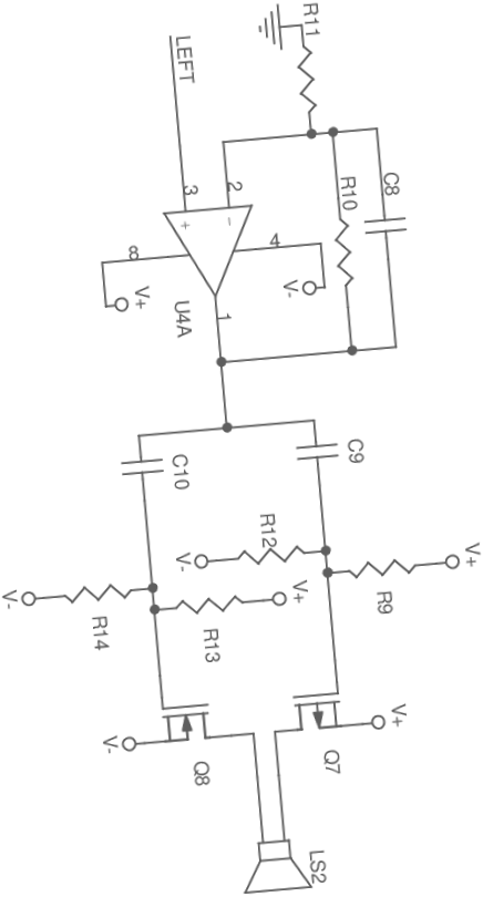
A switching power supply for producing +/-12V from an unregulated input.
The above switching supply was one of six regulators used in one design. The design is very compact, and uses off-the-shelf switching magnetics to produce an affordable supply.
So what’s notable?
- The input voltage signal VRAW enters from the left, while the output voltages, ±12V, are shown on the right.
- The capacitors on the input are shown with the smaller capacitance (C170) closer than the bigger one. The same arrangement is shown on the output side (C167 and C173). Smaller capacitors have a higher self-resonant frequency and should be closer to the noise source they filter. This is a subtle point and may not require explanation to the customer, but it’s a strong hint when layout commences. Eventually, the concept becomes a physical reality, and hints for layout are invaluable.
- Analogue connections are shown with full wires, but not all of them. The column of resistors on the far right, R96 R98 R99 R100, set the feedback voltages required by the regulator to produce the desired ±12V output voltages. The two nets, FB1372 and NFB1372, are feedback connections to the regulator, but drawing full traces from the resistors to D30, D33 and the feedback pins on U42 would hurt readability.
- The digital signal, SYNC, is a clock used to clock all regulators simultaneously, but rather than show a trace meandering all over the page, it’s much clearer to just put a small stub on the pin.
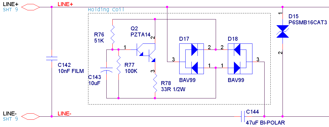 A shunt-current regulator typically found in fax/modem interfaces.
A Direct Access Arrangement (DAA) employed in telephone sets and fax/modem cards is shown above. A circuit similar to this can be found in virtually any device that connects to the telephone system at customer premises. The contents inside the dashed line with “Holding Coil” written above it represent a shunt or fixed-current regulator. These types of interfaces draw a consistent amount of current, indicating to a Central Office (CO) that the telephone set (or fax machine, or modem) is off-hook and requires a communication channel. Though a fixed amount of DC current is drawn, the circuit presents a virtually infinite impedance to AC, which means when analogue or voice data is transmitted through the telephone system, none of that signal energy is lost to the above regulator.
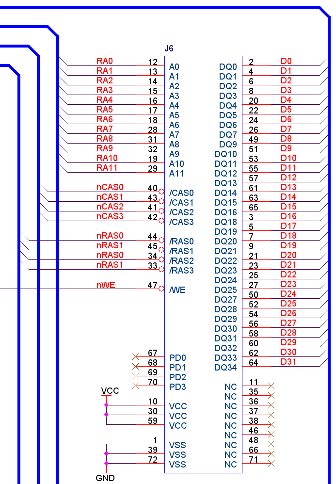
At left is a portion of an 80-pin flash SIMM designed into the Cirrus Logic CL-PS7500FE evaluation board. This design pre-dates the availability of flash SD cards, however it illustrates schematic capture as a form of communication.
The flash SIMM was chosen as a means of permitting developers to employ as much or as little flash memory as required during development. An additional advantage of the flash SIMM is that a ROM emulator could be plugged into the socket. This permitted development without burning application code into memory.
J-Tech currently uses OrCAD Capture to meet customer requirements. Capture is able to produce output suitable for import into most layout editors. Other tools are employed as needed: CADStar, Eagle, and KiCAD, to name a few.
Importing designs from competing schematic capture tools such as Altium is possible, however this tends to be nearly as much work as starting over. The single biggest problem is that library components don’t have the same names from one CAD package to another.
Please direct inquiries regarding designing with OrCAD (or any other schematic editor) to J-Tech Engineering. Contact information can be found on the company information page.